
Creating a PCB layout is a crucial step in the design of electronic circuits, impacting everything from performance to manufacturability. Understanding the intricacies of layout design not only helps in achieving optimal functionality but also saves time and resources during production. This article dives into essential techniques and best practices for crafting effective PCB layouts, ensuring your designs stand out in a competitive landscape.
Understanding PCB Layout Basics
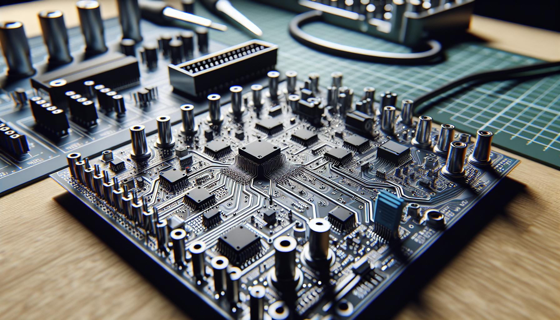
PCB layout design forms the foundation of electronic circuit development. Knowledge of essential principles can significantly impact device performance and production efficiency.
What is a PCB Layout?
A PCB layout refers to the arrangement of electronic components and the connections between them on a printed circuit board. It determines the placement of resistors, capacitors, integrated circuits, and traces that create electrical pathways. Effective layout design ensures optimal signal integrity, minimizes interference, and supports manufacturing processes.
For those seeking professional assistance, utilizing OurPCB printed circuit board layout services can ensure precision and efficiency in PCB design, especially for complex or high-speed applications.
Importance of PCB Layout in Electronics
PCB layout plays a critical role in electronics. It affects circuit functionality, reliability, and manufacturability. Key factors include:
- Signal Integrity: Proper trace routing minimizes noise and electromagnetic interference, maintaining signal quality.
- Thermal Management: Strategic component placement aids heat dissipation, enhancing device longevity.
- Manufacturing Efficiency: A clear layout reduces assembly complexity, lowering production costs and time.
- Design Validation: Well-structured layouts simplify testing and debugging, streamlining the development cycle.
Understanding these aspects of PCB layout is vital for designers aiming to create high-quality electronic products.
Tools and Software for PCB Design

Selecting the right tools and software for PCB design can significantly impact the design process. Several options cater to different skill levels and project requirements.
Popular PCB Design Software
- Altium Designer: Altium Designer is widely recognized for its user-friendly interface and powerful design capabilities. It supports high-speed designs and features extensive libraries and collaboration tools.
- Eagle: Eagle is a popular choice among hobbyists and professionals alike. Its functionality includes schematic capture, PCB layout, and a large component library, making it suitable for small to medium projects.
- KiCAD: KiCAD is an open-source PCB design tool that offers comprehensive features, including schematic design and 3D modeling. It appeals to users looking for a free yet robust solution.
- OrCAD: OrCAD provides advanced design and simulation tools, such as SPICE simulation and integrated circuit design. It’s favored in professional environments where precision and validation are critical.
- PADS: PADS emphasizes PCB design for high-speed and complex applications. It includes capabilities for design verification and thermal analysis, making it suitable for demanding projects.
Features to Look For in PCB Software
- User Interface: An intuitive user interface enhances productivity. Look for software with easy navigation and accessibility to essential tools.
- Schematic Capture: Efficient schematic capture allows users to create designs quickly. Look for software that facilitates straightforward drawing and editing of circuits.
- PCB Layout Capabilities: High-quality layout tools support optimal component placement and routing. The software should allow for automatic routing and design rule checks.
- 3D Visualization: 3D visualization assists in understanding layout and component placement in a physical space. This feature helps identify potential design issues early.
- Collaborative Features: Collaboration tools enable teams to work together on designs. Software should support real-time sharing and editing.
- Library Management: Extensive libraries for components can streamline the design process. Consider software that includes readily available or customizable component libraries.
- Support and Community: Reliable support and an active community can improve the user experience. Look for software with comprehensive documentation and forums for assistance.
These tools and features facilitate efficient and effective PCB design, supporting engineers in achieving high-quality results.
Step-by-Step Guide on How to Create a PCB Layout
Creating an efficient PCB layout requires meticulous planning and execution. Follow these steps to ensure a well-structured and functional design.
Designing the Schematic
Designing the schematic represents the foundational step in PCB creation. Start by defining the circuit behavior using symbols for components such as resistors, capacitors, and integrated circuits. Use software to integrate these components into a cohesive schematic diagram. Verify connections and functionality by simulating the circuit, ensuring it operates as intended. Accurate schematics prevent errors during the layout stage.
Placing Components
Placing components effectively on the PCB influences the overall performance. Begin by arranging components according to the schematic positions. Position components close to their related connections to minimize trace length. Group similar components together to simplify routing and improve signal integrity. Ensure adequate space around components for soldering and thermal dissipation. Using guidelines, such as manufacturer recommendations for component placement, contributes to a more efficient design.
Routing Traces
Routing traces involves establishing electrical connections between components. Start with critical signal pathways, ensuring they remain as short and direct as possible. Utilize wide traces for high-current paths to reduce resistance and heating issues. Implement ground planes when needed to improve signal integrity and reduce noise. Maintain appropriate spacing between traces to prevent unintentional short circuits. After routing, check for design rule violations to ensure manufacturability and reliability. Optimize the layout by reviewing trace routing for efficiency and performance.
Best Practices for PCB Layout
Creating an effective PCB layout requires attention to detail and adherence to best practices. Focused implementation of these practices enhances functionality and efficiency.
Minimizing Interference
Minimizing interference ensures optimal performance in PCB design. Designers should:
- Separate Analog and Digital Signals: Place analog and digital components on different areas of the PCB to reduce crosstalk.
- Employ Ground Planes: Use ground planes to shield sensitive circuits. Continuous ground layers help reduce electromagnetic interference.
- Utilize Signal Traces Wisely: Route signal traces away from potential noise sources. Short, direct paths minimize inductance and capacitance.
- Implement Differential Pairs: Use differential pairs for high-speed signals. This approach cancels out noise and enhances signal integrity.
Ensuring Manufacturability
Ensuring manufacturability supports production efficiency and quality. Important practices include:
- Follow Design Rules: Adhere to specific design rules for trace width, spacing, and pad sizes based on manufacturing capabilities.
- Use Standard Component Sizes: Select standard component sizes to simplify sourcing and assembly processes. Avoid custom parts unless necessary.
- Incorporate Test Points: Add test points for critical signals. These facilitate testing and debugging, ensuring successful assembly.
- Optimize Layer Stackup: Design a layer stack that meets electrical performance and manufacturability criteria. Balance layer counts for cost and complexity.
Adhering to these best practices results in robust PCB layouts, enhancing both performance and manufacturability in electronic products.
Common Mistakes to Avoid in PCB Layout
Mistakes in PCB layout can significantly impact performance, reliability, and manufacturability. Understanding these common errors helps designers avoid pitfalls during the design process.
Overcrowding Components
Overcrowding components on a PCB can lead to numerous issues. It can cause thermal problems due to insufficient airflow, complicate soldering processes, and hinder troubleshooting efforts. Designers must space components appropriately, ensuring enough room for heat dissipation and easy access for maintenance. A minimum clearance of 2-3mm between components is recommended to facilitate airflow and prevent heat accumulation.
Ignoring Ground Planes
Ignoring ground planes can result in poor signal integrity and increased susceptibility to noise. Ground planes provide a return path for signals and help reduce electromagnetic interference (EMI). Designers should utilize solid ground planes instead of thin traces, ensuring better grounding and reduced voltage fluctuations. Implementing ground planes properly enhances overall PCB performance.
Conclusion
Creating an effective PCB layout is essential for any electronic project. By mastering design techniques and utilizing the right tools, designers can significantly improve both performance and manufacturability. Attention to detail and adherence to best practices are crucial for avoiding common mistakes and ensuring optimal signal integrity.
As the industry continues to evolve, staying informed about the latest software and design strategies will empower engineers to produce high-quality electronic products. With a solid understanding of PCB layout principles, designers are well-equipped to thrive in a competitive market.
Frequently Asked Questions
What is PCB layout design?
PCB layout design refers to the arrangement of electronic components and their connections on a printed circuit board. It plays a crucial role in ensuring optimal performance, manufacturability, and signal integrity for electronic devices.
Why is PCB layout important?
PCB layout is vital because it affects the performance and manufacturability of electronic circuits. A well-designed layout minimizes interference, enhances signal integrity, and ensures efficient production processes.
What are the key factors in PCB layout?
Critical factors in PCB layout include signal integrity, thermal management, manufacturing efficiency, and design validation. These elements influence the overall quality and reliability of electronic products.
What software is best for PCB design?
Popular PCB design software includes Altium Designer, Eagle, KiCAD, OrCAD, and PADS. The best choice depends on your skill level, project requirements, and desired features like schematic capture and 3D visualization.
How do I create an effective PCB layout?
To create a PCB layout, start by designing the schematic, then place components strategically, ensuring related connections are close together. Finally, route traces to establish electrical connections, keeping pathways short and properly spaced.
What are common mistakes to avoid in PCB layout?
Common mistakes in PCB layout include overcrowding components, not maintaining adequate clearance for proper airflow, and neglecting the use of ground planes. These errors can lead to thermal issues and signal integrity problems.
How can I enhance signal integrity in my PCB design?
Enhancing signal integrity can be achieved by separating analog and digital signals, using ground planes, employing wisely routed signal traces, and implementing differential pairs for high-speed signals.
What best practices should I follow for PCB layout?
Best practices for PCB layout include adhering to design rules, avoiding overcrowding, using standard component sizes, incorporating test points, and optimizing layer stackup for better performance and manufacturability.